So, here it comes. I need a small, pretty looking PCB for the infrared switcher.
It took 3 hours to validate the order, almost 25 hours to make the PCBs and almost 2 days to announce them delivery ready.
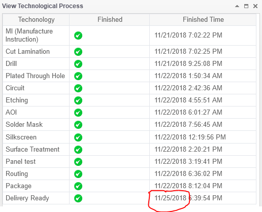
To be continued, once they arrive 🙂
Nov 25
So, here it comes. I need a small, pretty looking PCB for the infrared switcher.
It took 3 hours to validate the order, almost 25 hours to make the PCBs and almost 2 days to announce them delivery ready.
To be continued, once they arrive 🙂
Sometimes I find myself in awkward situations.
Some time ago we have installed a video duplication system in one of auditoriums. It is based on the HDMI backbone and some active equipment, like splitters and media converters.
It has single video injection point, where different sources can be selected. Source switching is made using KD-S4X1 switch from Key Digital.
One small problem is the entire installation must be concealed, while the switch is controlled with a button on the case and the IR remote. It has also no means of displaying the output, except a LED per active channel.
And so the Project was born: place a push button anywhere and replay the sequence on the IR LED inside the enclosure. Just to be sure, an Read the rest of this entry »
Apr 15
A scrap piece of 5+ year old UV sensitive PCB. The sticky black residue on the PCB is the clue from the protective foil.
Transparent foil for laser printers. Printed on Samsung CLP-320 in greyscale mode. Single layer.
The rest of the PCB will be used for the rectifier circuit. Read the rest of this entry »