The PCB:
A scrap piece of 5+ year old UV sensitive PCB. The sticky black residue on the PCB is the clue from the protective foil.
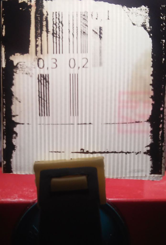
The mask:
Transparent foil for laser printers. Printed on Samsung CLP-320 in greyscale mode. Single layer.
The traces:
- 0,1 mm with the gap of 0,1 mm
- 0,1 mm with the gap of 0,2 mm
- 0,2 mm with the gap of 0,2 mm
- 0,2 mm with the gap of 0,3 mm
- 0,2 mm with the gap of 0,4 mm
- 0,3 mm with the gap of 0,2 mm
- 0,3 mm with the gap of 0,3 mm
- 0,2 mm with the gap of 0,6 mm
The rest of the PCB will be used for the rectifier circuit.
The UV cycle:
- preheat lamps for 3 minutes
- exposure for 6 minutes
The developer:
DP 50 (probably 🙂 @ 20°C, no agitation
Rinse
Use running water.
After the developing, traces of 0,1/0,1 mm are seen as solid.
 But not at the larger scale:
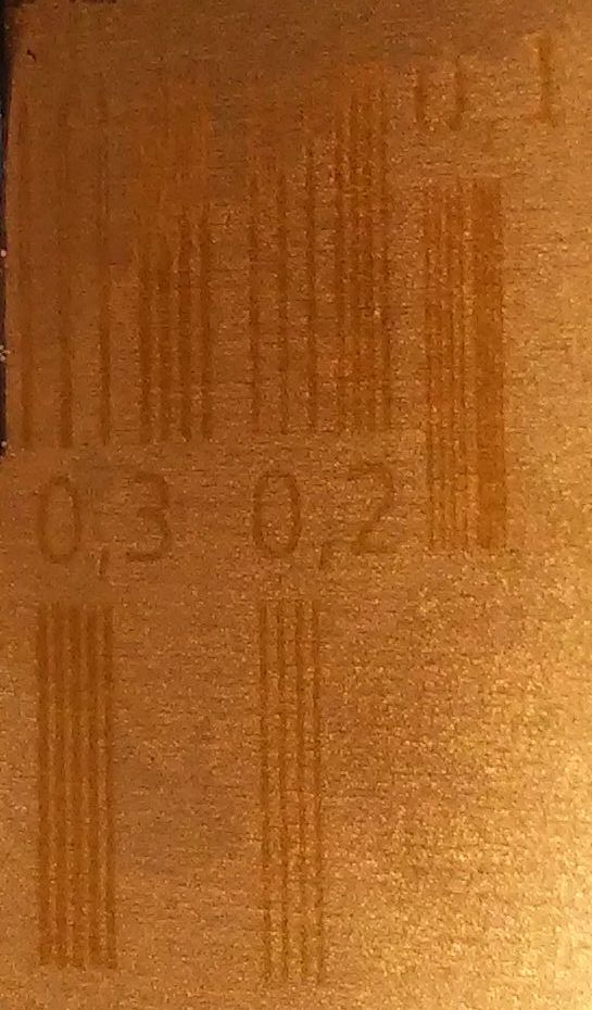
Seem like PCB got some unintentional light on the upper left corner?
Etcher:
Sodium persulfate @ 25°C, constant manual agitation. Too cold, thus took too long to etch the copper layer.
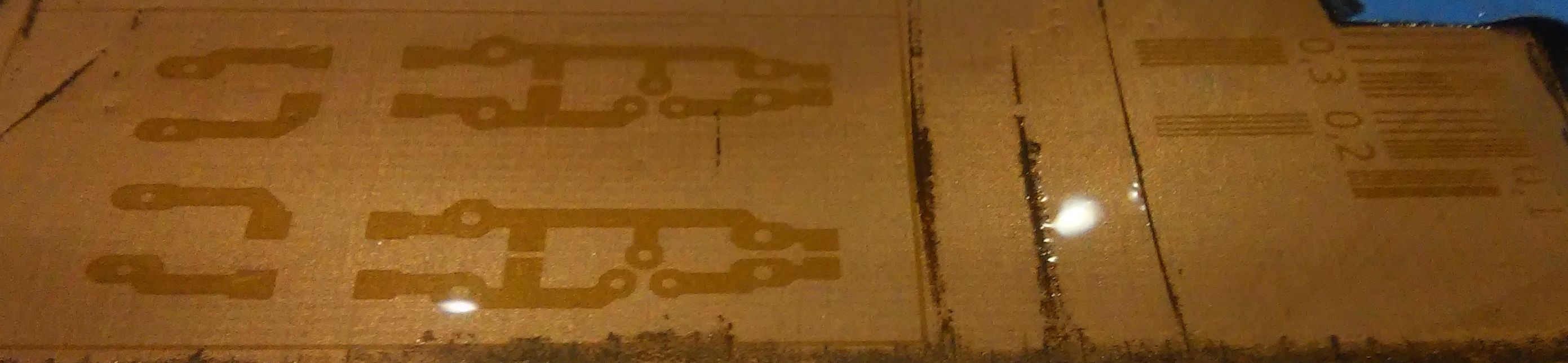
After the etch bath:
Definitely there is a problem with the transparent exposure pad. Scratches are all over the upper traces.
- traces of 0,1 / 0,1 mm are not continuous and too narrow;
- traces of 0,1 / 0,2 mm are not continuous and too narrow;
- traces of 0,2 / 0,2 mm are too narrow;
- traces of 0,2 / 0,3 mm are too narrow but almost perfect;
- traces of 0,2 / 0,4 mm are too narrow;
- traces of 0,3 / 0,2 mm are too narrow but of acceptable quality;
- traces of 0,3 / 0,3 mm are slightly “washed out” but of acceptable quality;
- traces of 0,3 / 0,6 mm are of different widths and slightly “washed out”;
Rants:
- Get rid of the current exposure plate.
- Preheat the developer up to 20-25°C and keep the temperature constant;
- Preheat the etcher up to 40-42°C and keep the temperature constant. Are there any indirect heaters available?
- Agitate the etcher. Need to search for magnetically coupled plastic pump on the eBay.
- Place a mate UV unifying media between the lamps and the PCB.
- Clean the PCB after removing the foil. The glue stick everywhere …
- Traces of 0,2/0,1 mm are worth trying. Expect them to appear as 0,15/0,15 mm on the PCB. For this i will need constant and turbulent agitation system. Laminar flow will probably overetch the parallel traces.